Lithography, a printmaking technique using a plate or other hard, smooth surface to transfer ink onto a medium such as paper, was invented in the late 18th century by German playwright Alois Senefelde. It is used to create a myriad of products, many sitting around your home and office.
But what if you needed to create something really small using lithographic techniques, even as small as the nanometer level, which is one billionth of a meter?
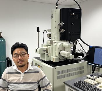
Ethan Ahn, an associate professor of electrical engineering at George Mason University, is doing research using a new technique called electron-beam lithography (EBL), which scans a focused beam of electrons to draw shapes. In fact, as the only skilled practitioner at Northern Virginia’s only EBL facility—in the university’s Nanofabrication Facility on the Science and Technology Campus in Manassas—he’s an evangelist for the technique, eager to get students and other faculty members trained on the technology.
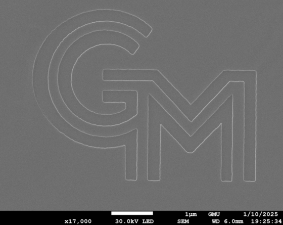
“This equipment is infamous for its sensitivity,” he said. “It’s a hard tool to use and it takes a lot of practice, a lot of training, and a lot of knowledge. So, this is not something that’s easily accessible to everyone.”
In fact, before Ahn’s arrival in 2023, students and faculty who wanted to work on EBL had to go to the National Institute of Standards and Technology campus in Gaithersburg, Maryland, more than an hour away from SciTech. Ahn is eager to train students and others to use the EBL technology, envisioning allowing time for researchers both within and outside of George Mason to tinker with the tiny-making toy.
“We will be able to get grants and funding that we wouldn't without this technology, absolutely,” said Ahn, about the possibilities EBL opens up. “And there’s an implication for myself, for example, because I'm working on nano electronics, and this will let us make nanoscale logic devices, nanoscale memory devices, and more.”
Ahn pointed to the microchip industry as a place where lithographic patterning is used extensively. Holding one up he said, “One small chip is as small as my thumb. But if you zoom in to see what is in there until you see individual devices and components, you’ll see billions of transistors there. That’s what I do for my research, making such devices using EBL, with transistors that are faster, more energy efficient, more reliable, and more secure.”
And students coming through Ahn’s EBL boot camp may find a future that is more secure, as they will be more marketable upon graduation, particularly in the high-tech hub that is the Washington, D.C., area.
Funding to support the EBL capability came from the GO Virginia Nano-IMAGINE program.
In This Story
Related News
- February 24, 2026
- September 14, 2025
- February 3, 2025
- May 17, 2024
- April 9, 2024